
What are Through Silicon Vias?

Review: TSVs
Three-dimensional integrated circuit (3D IC) and 2.5D IC
with Si interposer are regarded as promising candidates to overcome the
limitations of Moore’s law because of their advantages of lower power
consumption, smaller form factor, higher performance, and higher function
density. To achieve 3D and 2.5D IC integrations, several key technologies are
required, such as through-silicon via (TSV), wafer thinning, and handling, as
well as wafer/chip bonding. Since TSV provides the advantages of shortening
interconnection paths and thinner package size, it is considered as the heart
of 3D integration. TSV formation is categorized into three types during 3D/2.5D
IC process. When TSV is formed before CMOS processes, the process progression
is defined as via first. In via middle flow, backend process only continues
after the completion of TSV process. The final scheme is via last where TSV is
fabricated from the front side or back side of wafer after completing the CMOS
processes.
The choice of TSV schemes is based on the final application requirement in the semiconductor industry. TSV technology has been developed for many applications, such as MEMS, mobile phone, CMOS image sensor (CIS), bio application devices, and memory products. Thus, a number of studies have been conducted on the manufacturing of TSV. In current status, with the relatively high fabrication cost, TSV implementation in 3D IC and advanced packaging applications is not generally implemented yet. In this paper, we review the important manufacturing processes of TSV and related failure modes when TSV has a smaller diameter and higher aspect ratio. Furthermore, TSV fabrication has various important processes, including via formation by deep reactive ion etching (DRIE), lining with dielectric layer, barrier and seed layers, via filling, chemical mechanical polishing (CMP), and Cu revealing process. Each key technique will be introduced in detail in the following sections.
Benefits
While traditional CMOS scaling
processes improves signal propagation speed, scaling from current manufacturing
and chip-design technologies is becoming more difficult and costly, in part
because of power-density constraints, and in part because interconnects do not
become faster while transistors do. 3D ICs address the scaling
challenge by stacking 2D dies and connecting them in the 3rd dimension. This
promises to speed up communication between layered chips, compared to planar
layout. 3D ICs promise many significant benefits, including:
Footprint
More functionality fits into a
small space. This extends Moore's law and enables a new generation of
tiny but powerful devices.
Cost
Partitioning a large chip into
multiple smaller dies with 3D stacking can improve the yield and reduce the
fabrication cost if individual dies are tested separately.
Heterogeneous integration
Circuit layers can be built with
different processes, or even on different types of wafers. This means that
components can be optimized to a much greater degree than if they were built
together on a single wafer. Moreover, components with incompatible
manufacturing could be combined in a single 3D IC.
Shorter interconnect
The average wire length is
reduced. Common figures reported by researchers are on the order of 10–15%, but
this reduction mostly applies to longer interconnect, which may affect circuit
delay by a greater amount. Given that 3D wires have much higher capacitance
than conventional in-die wires, circuit delay may or may not improve.
Power
Keeping a signal on-chip can
reduce its power consumption by 10–100 times. Shorter wires also
reduce power consumption by producing less parasitic capacitance. Reducing
the power budget leads to less heat generation, extended battery life, and
lower cost of operation.
Design
The vertical dimension adds a
higher order of connectivity and offers new design possibilities.
Circuit security
3D integration can achieve security
through obscurity; the stacked structure complicates attempts to reverse
engineer the circuitry. Sensitive circuits may also be divided among the
layers in such a way as to obscure the function of each layer. Moreover,
3D integration allows to integrate dedicated, system monitor-like features
in separate layers. The objective here is to implement some kind of
hardware firewall for any commodity components/chips to be monitored
at runtime, seeking to protect the whole electronic system against
run-time attacks as well as malicious hardware modifications.
Bandwidth
3D integration allows large numbers of vertical vias between the layers. This allows construction of wide bandwidth buses between functional blocks in different layers. A typical example would be a processor+memory 3D stack, with the cache memory stacked on top of the processor. This arrangement allows a bus much wider than the typical 128 or 256 bits between the cache and processor. Wide buses in turn alleviate the memory wall problem.
The Benefits of 3D ICs: in other words
3D ICs offer many benefits over conventional,
large-area SoCs, most of which stem from
shortening the interconnect. With functional blocks stacked on top of each
other and connected through TSVs as opposed to long wires like in a 2D SoC, 3D
ICs are able to significantly decrease interconnect length.
Most notably, decreasing the
interconnect length helps alleviate parasitic impedances in the interconnect,
which in turn allows for decreased propagation delay (i.e faster operation) and
less data movement energy (i.e. less power consumption).

The other obvious benefit of 3D ICs is the ability to densely integrate large functionality into smaller areas, offering a good alternative to the end of Moore’s law. It’s worth noting that this dense integration also comes with drawbacks such as increased power density and thermal management issues.
What’s the Catch?
If 3D is so wonderful, why isn’t everybody doing it?
There are a few major hurdles to overcome. First,
every die in the stack must be designed for stacking, and that design effort is
considerable. If different entities are responsible for the different
layers, close collaboration is essential from initial design through final
test. Second, the manufacturing steps must be carefully
coordinated. Different layers can be processed by different manufacturers,
and they are most likely stacked at yet another facility.
In specific markets such as memories and sensors, the
immediate benefits of 3D far outweigh the difficulties. Successes in
these initial markets are already establishing precedents for future
designs. As the 3D architecture matures, the industry will see a steady
increase in ambitious, ground-breaking 3D projects. 3D is clearly the
technology of the future!
Today, only a select few companies have mastered 3D. They have built the necessary relationships, created the supply chain, acquired the skills and experience, and actually produced working 3D ICs.
Challenges
Because this technology is new,
it carries new challenges, including:
Cost
While cost is a benefit when
compared with scaling, it has also been identified as a challenge to the
commercialization of 3D ICs in mainstream consumer applications. However,
work is being done to address this. Although 3D technology is new and fairly
complex, the cost of the manufacturing process is surprisingly straightforward
when broken down into the activities that build up the entire process. By
analyzing the combination of activities that lay at the base, cost drivers can
be identified. Once the cost drivers are identified, it becomes a less
complicated endeavor to determine where the majority of cost comes from and,
more importantly, where cost has the potential to be reduced.
Yield
Each extra manufacturing step
adds a risk for defects. In order for 3D ICs to be commercially viable,
defects could be repaired or tolerated, or defect density can be improved.
Heat
Heat building up within the stack
must be dissipated. This is an inevitable issue as electrical proximity
correlates with thermal proximity. Specific thermal hotspots must be more
carefully managed.
Design complexity
Taking full advantage of 3D
integration requires sophisticated design techniques and new CAD tools.
TSV-introduced overhead
TSVs are large compared to gates
and impact floor plans. At the 45 nm technology node, the area footprint
of a 10μm x 10μm TSV is comparable to that of about 50 gates. Furthermore,
manufacturability demands landing pads and keep-out zones which further
increase TSV area footprint. Depending on the technology choices, TSVs block
some subset of layout resources. Via-first TSVs are manufactured before
metallization, thus occupy the device layer and result in placement obstacles. Via-last
TSVs are manufactured after metallization and pass through the chip. Thus, they
occupy both the device and metal layers, resulting in placement and routing
obstacles. While the usage of TSVs is generally expected to reduce wire length,
this depends on the number of TSVs and their characteristics. Also, the
granularity of inter-die partitioning impacts wire length. It typically
decreases for moderate (blocks with 20-100 modules) and coarse (block-level
partitioning) granularities, but increases for fine (gate-level partitioning)
granularities.
Testing
To achieve high overall yield and
reduce costs, separate testing of independent dies is essential. However,
tight integration between adjacent active layers in 3D ICs entails a
significant amount of interconnect between different sections of the same
circuit module that were partitioned to different dies. Aside from the massive
overhead introduced by required TSVs, sections of such a module, e.g., a
multiplier, cannot be independently tested by conventional techniques. This
particularly applies to timing-critical paths laid out in 3D.
Lack of standards
There are few standards for
TSV-based 3D IC design, manufacturing, and packaging, although this issue
is being addressed. In addition, there are many integration options being
explored such as via-last, via-first, via-middle; interposers or
direct bonding; etc.
Heterogeneous integration supply chain
In heterogeneously integrated
systems, the delay of one part from one of the different parts suppliers delays
the delivery of the whole product, and so delays the revenue for each of the
3D IC part suppliers.
Lack of clearly defined ownership
It is unclear who should own the 3D IC integration and packaging/assembly. It could be assembly houses like ASE or the product OEMs.
Cooling Methods in 3D Integrated Circuits
Micro channels can be integrated into a 3D IC chip stack as a cooling interlayer. These layers can be placed between each of the chips of the IC, or after each of the two or more chips. The challenge of micro channel cooling is to integrate it with TSVs. The TSVs can only be located at the walls of the channel, and a large number of closely spaced micro channels are therefore desired. The desirable channel sizes in combination with the need for short TSV distances, tend to be brief and narrow micro channels. Such channels will produce high heat transfer efficiency due to small hydraulic diameters, but the pressure of the coolant stream falls through these channels becomes prohibitively excessive. Micro channels are generally classified in the range of 10–200μm as channels with a minimum element. In the case of conduction cooling, either the microchannels are placed directly in the silicon substratum or etched or machined in a separate silicon or copper chip connected to the back of the IC chip. These passages can also be etched between the interlayer in 3D ICs. A microchannel-cooled 3-layer 3D IC structure can also etch these passages between the interlayer in 3D ICs.
The Economics of 3D printing ICs
In any
manufacturing process, the cost structure involved in manufacturing is an
important driver of the price of a finished device. Integrated circuits succeed
or fail based on the cost of the die on the wafer—when more dies can be placed
on a single wafer, the costs per device decreases. The cost structure of
integrated circuit manufacturing is responsible for the high costs of highly
specialized, low-volume integrated circuits. An excellent example can be found
in the defense industry, where the cost of a single FPGA for a complex system
can reach tens of thousands of dollars.
The unique cost structure of 3D printed devices changes this economic dynamic. 3D printed integrated circuits do not need to be produced on a wafer and can even be manufactured individually. Because 3D printed devices can be produced with predictable fabrication time, and the cost structure is complexity agnostic, the costs involved in 3D printing electronics depends on the weight of the materials used. This makes 3D-printed integrated circuits highly cost competitive for low-volume production compared to devices produced on semiconductor wafers with standard processes.
Test and Design-for-Testability Solutions for Monolithic 3D Integrated Circuits
Three-dimensional (3D)
integration is a promising way to sustain Moore's Law beyond device- and
interconnect-scaling limits. 3D technologies enable the integration of
heterogeneous fabrication processes, and provide high-speed interconnects, high
device-integration density, and low power consumption. Today's 3D technologies
can broadly be classified into two categories based on the integration process:
(i) 3D die/wafer stacking, in which separately manufactured dies/wafers are
integrated onto the same package, and (ii) monolithic 3D (M3D) integration, in
which transistor layers are processed sequentially on the same wafer.
Through-silicon-vias (TSVs) are used to connect dies to each other in a 3D
stacked integrated circuit (IC). In contrast, M3D ICs use inter-layer-vias
(ILVs) of much smaller dimensions to connect a metal line in one transistor
layer to a metal line in another transistor layer.
TSV-based 3D stacked ICs can be
manufactured without requiring substantial changes to the existing fabrication
flow. Considerable research efforts have therefore been directed towards the
development of TSV-based 3D stacking technology, and products based on this
technology have been successfully introduced into the marketplace, e.g., the
AMD Fiji chip. However, the keep-out-zone (KOZ) required for TSVs and
limitations on the die alignment precision impose limits on the device
integration density that can be achieved using TSV-based 3D stacking. A minimum
KOZ of 3 um is required for ICs fabricated at the 20 nm technology node, and the
die alignment precision is currently limited to 0.5 um.
The above limitations on
integration density can be overcome by adopting M3D integration. High-density
integration in M3D is enabled by the alignment precision of ILVs, which is
determined by the lithography stepper accuracy and has been reported to be 10
nm for the 22 nm technology node. In addition, the size and pitch of an ILV are
typically one to two orders of magnitude smaller than those of a TSV.
Therefore, M3D integration can result in reduced area and higher performance
when compared to 3D die stacking.
Due to the above benefits of M3D
integration, there is a growing interest in industry towards the adoption of
this technology. However, test challenges for M3D integration have remained
largely unexplored. This thesis is focussed on four key test challenges for M3D
integration: (i) performance variations due to high-density integration, (ii)
defect analysis and modeling, (iii) defect isolation and yield enhancement, and
(iv) yield loss due to voltage droop. For each test challenge, we motivate the
need to study its impact on an M3D IC, analyze the effectiveness of existing
test solutions, and develop new solutions.
This dissertation first addresses
challenges (i) and (ii). We quantify the impact of electrostatic coupling and
wafer-bonding defects on the threshold voltage of a top-layer transistor in an
M3D IC. In addition, we show that wafer-bonding defects can lead to a change in
the resistance of ILVs, and in some cases, lead to an open in an ILV or a short
between two ILVs. We also study the impact of these defects on path delays and
on the effectiveness of delay-test patterns for large benchmarks. Our results
show that the timing characteristics of an M3D IC can be significantly altered
due to coupling and wafer-bonding defects if the thickness of its inter-layer
dielectric is less than 100 nm.
Next, this dissertation presents
a new DfT solution for M3D ICs based on dedicated test layers, which are
inserted between functional layers. We evaluate the cost associated with the
proposed DfT solution and compare it with that for a potential DfT solution
based on the proposed IEEE Std. P1838. Our results show that the proposed DfT
solution is more cost-efficient than the P1838-based DfT solution for a wide
range of ILV density, ILV yield, and defect density. We also present a test
scheduling and optimization technique for wafer-level testing of M3D ICs.
This dissertation then presents
an ILV BIST solution for M3D ICs to address isolation of ILV defects and yield
enhancement. In the proposed ILV BIST solution, interface-register cells in a
test layer are stitched into a TRC using their functional outputs and the ILVs.
We show that the proposed solution detects all hard opens and shorts in the
ILVs. We validate the detection of all hard opens and shorts using HSpice
simulations. We also implement an artificial neural network-based diagnosis
framework to estimate the size of ILV defect and show that the prediction
accuracy of the proposed framework is extremely high.
Finally, this dissertation
describes an optimization approach for reliable power delivery in M3D ICs to
address challenge (iv). We analyze the voltage droop during testing and compare
it with that observed during functional operation. We also quantify the impact
of voltage droop during testing on yield loss. Our results show that the
proposed power delivery optimization approach significantly reduces the
worst-case voltage droop and yield loss due to voltage droop compared to a
baseline.
In summary, the dissertation targets important design and optimization problems related to testing of M3D ICs. This research has led to theoretical insights, significant academic and industrial collaborations, simulations results using advanced process design kits, and a set of test and DfT solutions.
New package verification technologies
Similar to the PDKs used for a SoC, we are now seeing the
availability of 3D-IC package design kit elements developed and provided by
foundries and OSAT companies for multi-die processes. These initial
assembly-level design kits (ADKs) for packages typically include signoff
physical verification and connectivity verification (Figure 2). Physical
verification, by way of design rule checking (DRC), ensures that all the
components of the package are placed in a way that meets all the manufacturing
requirements. Connectivity verification includes, at a minimum, layout vs.
schematic (LVS) checking, parasitic extraction, and post-layout simulation. As
the 3D-IC market expands, additional verification functionality, such as
thermal and/or stress signoff solutions, can be added to the ADK.
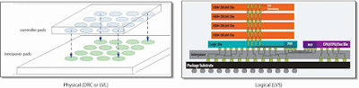
Figure 4. Package verification must include both physical
and connectivity checking.
Package designers also need validated technology files for
their design creation tools, just like those available for place and route
(P&R) and custom design tools in the IC space today. The critical aspect of
these files is layer mapping. Each element in a package design must map to the
proper assigned manufacturing layer to ensure the DRC and circuit verification
techniques work correctly.
The existence of these ADKs also enables electronic design
automation (EDA) companies to develop tools and automated process flows to help
package designers verify high-density advanced packages more quickly and
accurately, with the same sense of security that SoC designers enjoy today. To
be of true value across the industry, all of these processes must be
independent of any specific design tool used to create the assembly, and they
must be validated by the package assembly or OSAT Company.
Challenges of the 3D ICs:
This technology is relatively new and is still under
development and research. Thus it has a few drawbacks just like all developing
technologies.

Cost: The commercialization of the 3D ICs in the mainstream consumer application has been very challenging. What has been put for addressing this issue such that it can be scaled to a point that it can be profitable. The manufacturing cost of the 3D IC can be easily broken down into its stages of manufacture despite being such a new technology. After breaking down the cost in stages, the cost drivers can easily be identified and once they are identified, it can be easily defined where the majority of the cost is coming from and how it can be reduced.
Testing: Testing of the
individual layers is very important if we want to achieve a high yield overall
and reduce the cost. But due to the design of the 3D IC in which the adjacent
layers are tightly interconnected, it becomes very difficult to test the
individual layers separately. Due to being a 3D model, its circuit cannot
be tested by conventional means thus incurring additional overheads.
Few
Standards: Very
few standards exist for the 3D IC model in its manufacturing, designing, and
even packaging. Although this issue has been already addressed, very few
actions have been taken to solve this issue. The use of heterogeneous
integration supply chain is that the delay caused by the supplier of a
particular part causes a delay in the delivery of the whole product. This in
turn causes delays in the revenue generation of each product.
Yield: As we know every step
in manufacturing adds a chance of defect in the product. If we want the product
of 3D IC to be viable on a commercial basis, the defects that are caused should
be repairable or tolerable. The otherwise public commercial application would
be very costly.
Heat: The 3D IC is in the
form of a stack. In the design of a stack, heating is an inevitable issue
because the electrical proximity greatly correlates with thermal proximity. So
the heat that builds up must be dissipated and the thermal hotspots that exist
in the structure must be managed carefully.
Links:
https://en.wikipedia.org/wiki/Three-dimensional_integrated_circuit
https://www.sciencedirect.com/topics/engineering/three-dimensional-integrated-circuits
https://www.3dincites.com/3d-incites-knowledge-portal/what-is-3d-integration/
https://blog.bitsathy.ac.in/3-dimensional-or-3d-integrated-circuits/
https://nhanced-semi.com/technology/about-3d-ics/
https://www.nano-di.com/blog/2019-3d-printing-integrated-circuits-whats-possible-now-and-in-the-futurehttps://www.nano-di.com/blog/2019-3d-printing-integrated-circuits-whats-possible-now-and-in-the-future
https://dukespace.lib.duke.edu/dspace/handle/10161/18664
https://www.eetimes.com/is-3d-ic-the-next-big-profit-driver/https://www.eetimes.com/is-3d-ic-the-next-big-profit-driver/
https://blog.pooripadhai.com/what-do-we-mean-by-3d-integrated-circuits/
and
18 other pdf file references
For all discussed seminar
topics list click here Index.
…till next post, bye-bye and take care.


